Samsung Reportedly Working on Backside Power Supply Tech with 2 Nanometer Process
Mar 04, 2024
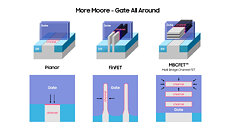
Lately, important industry figures have been hyping up Backside Power Supply Delivery Network (BSPDN) technology—recent Intel Foundry Services (IFS) press material lays claim to several technological innovations. A prime example being an ambitious five-nodes-in-four-years (5N4Y) process roadmap that: "remains on track and will deliver the industry's first backside power solution." A Chosun Business report proposes that Samsung is working on Backside Power Supply designs—a possible "game changer" when combined with in-house 2 nm SF2 GAAFET. Early experiments, allegedly, involving two unidentified ARM cores have exceeded expectations—according to Chosun's sources, engineers were able to: "reduce the chip area by 10% and 19%, respectively, and succeeded in improving chip performance and frequency efficiency to a single-digit level." Samsung Foundry could be adjusting its mass production timetables, based on freshly reported technological breakthroughs—SF2 GAAFET + BSPDN designs could arrive before the original targeted year of 2027. Prior to the latest developments, Samsung's BSPDN tech was linked to a futuristic 1.7 nm line.


View at TechPowerUp Main Site | Source